ADC Introduction
The ADC subsystem consists of a signal multiplexer and a voltage analog-to-digital converter (VADC), which is designed to route internal and external analog signals to the VADC via multiplexing and complete the conversion from analog quantities to digital quantities.
ADC Module hardware Architecture Diagram
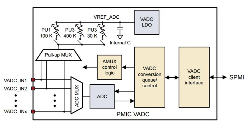
ADC supported by the module
M1 The ADCs supported by the module are as follows:
Interface |
Pin Number |
Pin Name |
PM4250 Pin Number |
Voltage Domain |
MPM Interrupt |
Pin Description |
|---|---|---|---|---|---|---|
ADC |
128 |
ADC0 |
GPIO4 |
1.8 V |
- |
PMU_GPIO04 |
ADC |
185 |
ADC1 |
GPIO7 |
1.8 V |
- |
PMU_GPIO07 |
L1 The ADCs supported by the module are as follows:
Interface |
Pin Number |
Pin Name |
PM4250 Pin Number |
Voltage Domain |
MPM Interrupt |
Pin Description |
|---|---|---|---|---|---|---|
ADC |
128 |
ADC0 |
PMU_GPIO06 |
1.8 V |
- |
PMU_GPIO04 |
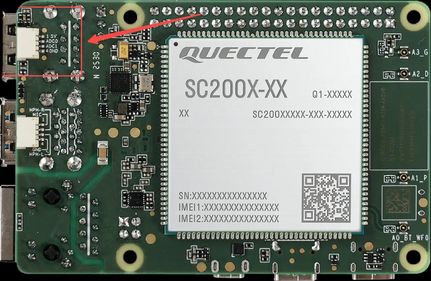
M1/L1 ADC position
The position of the ADC interface on the intelligent main control board is shown in the following figure:
Usage Example of ADC Node
The ADC node is mainly used to view the ADC value input to this node.
Instructions for use
An adjustable DC power supply shall be used as the input signal source during the test:
Connect the power supply positive terminal to the ADC0 or ADC1 pin.
Power supply GND is connected to the GND of the intelligent main control board.
M1: The corresponding relationship of each channel and input characteristics are as follows:
ADC0:
Connect to GPIO4
节点:
in_voltage_adc_gpio4_inputSupported input voltage range: approx. 0~5.25 V
ADC1:
Connect to GPIO7
节点:
in_voltage_adc_gpio7_inputSupported input voltage range: approx. 0~5.25 V
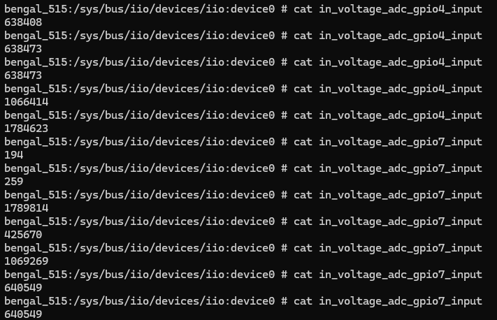
After setting the output of the DC power supply to the target voltage, the ADC sampling result (unit: μV) can be read via the following command:
adb shell
cd /sys/bus/iio/devices/iio:device0
cat in_voltage_adc_gpio4_input
cat in_voltage_adc_gpio7_input
L1: The channel correspondence and input characteristics are as follows:
ADC0:
Connect to PMU_GPIO6
节点:
in_voltage_adc_gpio6_inputSupported input voltage range: approx. 0~5.25 V
After setting the output of the DC power supply to the target voltage, the ADC sampling result (unit: μV) can be read via the following command:
adb shell
cd /sys/bus/iio/devices/iio:device1
cat in_voltage_adc_gpio6_input
Test Code
The following sample code demonstrates the basic method of reading ADC voltage values in an application. The program reads the raw ADC value (in μV) by accessing the node file corresponding to the ADC, and converts it into an integer for subsequent processing.
Click to expand/collapse: ADC reading test code (can be compiled via NDK by yourself)
#include <stdio.h>#include <stdlib.h>#include <unistd.h>#include <fcntl.h>#include <string.h>#include <errno.h>int main()
{
    int fd = -1;
    int adc_value;
    char buff[64] = {0};

    // Open the ADC node file (ADC0 corresponds to GPIO4)
    fd = open("/sys/bus/iio/devices/iio:device0/in_voltage_adc_gpio4_input", O_RDONLY);
    if(fd < 0){
        perror("open error\n");
        return fd;
    }

    // Read the ADC value int n_read = read(fd, buff, sizeof(buff));
    if(n_read < 0) {perror("read error\n");close(fd);return -1;}// Convert the read string into an integer (unit: μV)
    adc_value = atol(buff);
    printf("read %d bytes, content: %s\n", n_read, buff);
    printf("ADC value: %d μV\n", adc_value);

    close(fd);
    return 0;
}
#include <stdio.h>#include <stdlib.h>#include <unistd.h>#include <fcntl.h>#include <string.h>#include <errno.h>int main()
{
    int fd = -1;
    int adc_value;
    char buff[64] = {0};

    // Open the ADC node file (ADC0 corresponds to PMU_GPIO6)
    fd = open("/sys/bus/iio/devices/iio:device1/in_voltage_adc_gpio6_input", O_RDONLY);
    if(fd < 0){
        perror("open error\n");
        return fd;
    }

    // Read the ADC value int n_read = read(fd, buff, sizeof(buff));
    if(n_read < 0) {perror("read error\n");close(fd);return -1;}// Convert the read string into an integer (unit: μV)
    adc_value = atol(buff);
    printf("read %d bytes, content: %s\n", n_read, buff);
    printf("ADC value: %d μV\n", adc_value);

    close(fd);
    return 0;
}
Code Description:
Use
open ()function to open the ADC node file/sys/bus/iio/devices/iio: device0/in_voltage_adc_gpio4_input.Use
read ()function to read the raw ADC value (in string format, unit: μV).Use the
atol ()function to convert a string to a long integer value.The unit of the read ADC value is microvolts (μV), which can be converted into a voltage value as required.
Compile and run:
# Compile with NDK # Push the compiled executable file to the device and run it
adb push test_adc /data/local/tmp/test_adc
adb shell "chmod +x /data/local/tmp/test_adc"
adb shell "/data/local/tmp/test_adc"
Test Data
ADC Pin Specifications
The ADC pin definitions on the module are as follows:
Interface |
Module Pin Number |
Module Pin Name |
Module I/O |
NET Name (Multiplexing Function) |
Description |
|---|---|---|---|---|---|
ADC |
128 |
ADC0 |
I |
ADC0 |
1) Connector input voltage range: 0–5.25 V. 2) Voltage dividing resistors: RH = 18 kΩ, RL = 10 kΩ. 3) ADC pin voltage = connector input voltage (J0403) ×(10/28). 4) Example: When the input is 3 V, the voltage at the ADC pin shall be 3 V × 10/28 ≈ 1.0714 V. |
ADC |
185 |
ADC1 |
I |
ADC1 |
Same electrical characteristics as ADC0 (0–5.25 V input range, RH = 18 kΩ, RL = 10 kΩ, ADC pin voltage = Vin × 10/28). |
ADC0 Test Data
Voltage Source |
ADC0(μV) |
Theoretical Value (V) |
|---|---|---|
1.8 V |
638408 |
1.8 V×10/28 = 0.642857 |
3 V |
1066414 |
3 V×10/28 = 1.07143 |
5 V |
1784623 |
5 V×10/28 = 1.78571 |
ADC1 Test Data
Voltage Source |
ADC1(μV) |
Theoretical Value (V) |
|---|---|---|
1.8 V |
640549 |
1.8 V×10/28 = 0.642857 |
3 V |
1069269 |
3 V×10/28 = 1.07143 |
5 V |
1789814 |
5 V×10/28 = 1.78571 |